Commodore 128 Tips & Tricks
Herdware
Easter Egg - authors of Commodore 128:
SYS 32800,123,45,6
- this shows Commodore 128 designers team
Something for owner model C128D(CR)
Changing device number of internal C1571 of C128D (software method):
Type:
OPEN15,old,15
PRINT#15,"U0>"+CHR$(new)
CLOSE15
or
OPEN 1,8,15,"U0>"+CHR$(new):CLOSE 1
(old = old device number - standard 8, new = new device number, e.g. 9)
- change is temporary
Disabling disk drive:
OPEN 1,old,15,"M-W"+CHR$(119)+CHR$(0)+CHR$(2)+CHR$(0)+CHR$(0):CLOSE 1
- disabled is also temporary
Disable the built-in drive on your Commodore 128D
By Al Angor
===========================================
Okay, so you've installeddevice switches for the 1571 in your C128D.
Maybe you've also installed a momentary on switch to reset drive after changigng the device number (to replace the hard to use drive reset switch that comes with the D). What if you're lucky enough to have RAMLink, a CMD Hard Drive, a CMD FD-4000, and a C1581, and you'd like to use them with GEOS which has a limited number drives allowed? What if you'd like to not have internal drive recognized by your computer? With the faster, larger drives and RAM devices available, the 1571 in your C128D might need to be disabled now and then. Well folks, here's the answer.
Legal Mumbo Jumbo
-----------------------
Before we get started, a word of caution and a disclaimer. Inside your C128D are voltages which can harm you. Also, you can have static chargesin your body which can harm your C128D. If your unsure if you can complete this short project, get help from a friend, or go to a computer dealer/repair center. Neither Creative Micro Designs, Inc. nor the author of this article shall be responsible for the use or misuse of information in this article. The information provided has been tested and is believed to be correct. Now on to the fun stuff.
One more switch
-------------------
Here's the procedure for installing a drive disable switch on the front panel of the C128D.
Parts required for this job are:
- soldering pencil
- fine electronic solder
- 1 miniature toggle switch (spdt)
- 1 resister, 10K Ohm 1/4W
- 3ft. (approx.) of 28gauge stranded hookup wire
- a drill and bit to provide the hole to mount the switch in
- a small pair of diagonal cutters (nippers)
- an exacto knife
Lets get started. Open the C128D. Remove the screws from the rear and bottom of the unit. Slide the cover back, and remove it. Next, remove the 1571 drive unit. Remember the orientation of the connectors and remove them. Remove the drive mount screws and slide off the latch lever. Slide the drive unit out, and set it aside. If you've installed device selection switches before, all of this will be easy. If not, take your time and make notes.
One of the six lines in commodore famous (or infamous) serial bus is labeled ATN for "attention". This line is used to get the attention of all devices on serial bus. The host computer brings this line low, which in turn generates an interrupt on the drive controller board. The ATN signal is followed by device number. It works a little like a roll call. The computer calls all the serial devices to attention and looks for the device requested. If the device doesn't respond, the computer assumes it isn't there. You can switch the ATN line in and out for any serial device. I use a couple of rotary to allow me to select from a 1541, a 1571, and a 1581 as device 8, and the same for device 9. These rotary switches allow me to bring the ATN line to the drive of my choice. Our goal is to switch out the ATN line for the internal 1571 so it doesn't answer the roll call.
Enough theory, let's solder something! First, solder the resistor to one of the outside terminals on the switch. Next, cut the hookupwire into three equal sections of approximately 1 ft. each, strip the ends back about 1/16th of an inch, and solder one end of two of the wires to the two remaining terminals on the switch. Solder one end of the remaining wire to the open end of the resistor. Cut away any excess leads or wires so that your switch and resistorassembly looks like the one in the inset picture below.
Now refer to the picture and locate IC U1 on your C128D motherboard. This is a large (40 pin) 6526 chip near the right center of the board (shown at the far right in figure 2). Using IC U1 as a reference point, locate the threethrough-hole solder pads identified as Pads A, B and C in the picture. Notice that a trace runs between Pads A and C. Using an Exacto knife, cut this trace somewhere near Pad A (there's a little more clearance at that end of the trace). Make sure your cut creates a good solid break in the trace (you can verify this with an ohm-meter or continuity-checker if you have one). Now solder the wire connected to the center terminal of the switch to Pad A; solder the wire connected to the resistor to Pad B; finally, solder the remaining wire to Pad C.
Locate an appropriate location for mounting the switch on the front panel of your C128D, drill a hole, and mount the switch (you can feed the switch through one of the large holes in the metal frame of the C128D).
Reinstall the drive, and front panel if you removed it, and test your work. Then close up the C128D. If you close up the C128D before testing, something will be wrong and you'll need to reopen it (Murphy's Law being what it is.)
Wile E.Coyote
Detecting of computer model and mode
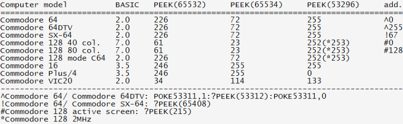
Detection of REAL Commodore 64 between Commodore 128 in C64 mode in assembler:
C128 test
LDA #$CC
STA $D030
LDA $D030
CMP #$FC (or $FD if is computer in 2MHz mode)
BEQ C128 in C64 mode
JMP real C64
8722 MEMORY MANAGEMENT UNIT DECLARATIONS
;
mmucr =$ff00 ;configuration...
;
; 0xxxxxxx
; |||||||
; ||||||+---> $D000-$DFFF: 0 = I/O hardware
; |||||| 1 = RAM or character ROM
; |||||+----> $4000-$7FFF: 0 = system ROM
; ||||| 1 = RAM
; |||++-----> $8000-$BFFF: 00 = system ROM
; ||| 01 = internal function ROM
; ||| 10 = external function ROM
; ||| 11 = RAM
; |++-------> $C000-$FFFF: 00 = system ROM
; | 01 = internal function ROM
; | 10 = external function ROM
; | 11 = RAM
; +---------> RAM bank: 0 = RAM-0
; 1 = RAM-1
;
lcra =mmucr+1 ;select configuration A
lcrb =mmucr+2 ;select configuration B
lcrc =mmucr+3 ;select configuration C
lcrd =mmucr+4 ;select configuration D
MEMORY MANAGEMENT C128
====================
Standard BANKs:
0 - RAM 0
1 - RAM 1
2 - RAM 0
3 - RAM 1
4 - Internal ROM/RAM 0/ I/O
5 - Internal ROM/RAM 1/ I/O
6 - Internal ROM/RAM 0/ I/O
7 - Internal ROM/RAM 1/ I/O
8 - External ROM/RAM 0/ I/O
9 - External ROM/RAM 1/ I/O
10 - External ROM/RAM 0/ I/O
11 - External ROM/RAM 1/ I/O
12 - KERNAL/Internal ROM(lo)/RAM 0/ I/O
13 - KERNAL/External ROM(lo)/RAM 0/ I/O
14 - KERNAL/BASIC ROM/RAM 0/Character ROM
15 - KERNAL/BASIC ROM/RAM 0/ I/O
Internal ROM - free EPROM socket for own EPROMs (think U36)
External ROM - free EPROM socket for own EPROMs on REU
-------------------------------------------
MMU - Memory Management Unit
========================
$ff00 = CR - configuration register
$ff01 = LCRA - load configuration register A
$ff02 = LCRB - load configuration register B
$ff03 = LCRC - load configuration register C
$ff04 = LCRD - load configuration register D
--------------------------------------------
parts of no-possible accessing MMU when is in BANK I/O (ff00-ff04 always visible)
$d500 = CR - configuration register
$d501 - PCRA - pre-configuration register A
$d502 - PCRB - pre-configuration register B
$d503 - PCRC - pre-configuration register C
$d504 - PCRD - pre-configuration register D
$d505 = MCR - mode configuration register
$d506 = RCR - RAM configuration register
$dc07 = P0L - page 0 pointer LO
$dc08 = P0H - page 0 pointer HI
$d509 = P1L - page1 pointer LO
$d50a - P1H - page 1 pointer HI
$d50b = VR - version register
---------------------------------------
CR - CONFIGURATION REGISTER
address $ff00 - $ff04 - always
address $d500 - $d504 - only if is in RAM I/O
CR bit 0 - 1 ROM HIGH (VIC/SID/MMU ($d500-$d50b)/CIA1/CIA2) = I/O
0 ROM HIGH in order of bit 4 and 5
- this bit sets area $d000 - $dfff)
default: 0
CR bit 1 - 1 RAM
- 0 BASIC LOW ROM
default 0
CR bit 2 - 3 = access to area $8000 - $bfff
1 / 1 = RAM
1 / 0 = Internal ROM
0 / 1 = External ROM
0 / 0 = BASIC ROM HIGH
default 0/0
CR bit 4 - 5 = access to area $c000 - $ffff
1 / 1 = RAM
1 / 0 = Internal ROM
0 / 1 = External ROM
0 / 0 = KERNAL/Charset ROM
default = 0/0
CR bit 6 - 7 = selecting of memory BANK
bit 7 = unused (only for cartridges)
bit 6 = 1 - RAM 1
bit 6 = 0 - RAM 0
All in one:
=======
7/6 5/4 3/2 1 0
BANK HI-SPACE MID-SPACE LO-SPACE I/O SPACE
SELECT ($c000-$ffff) ($8000-$bfff) ($4000-$7fff) ($d000-$dfff)
bit 7 - expansion bank
bit 7 / bit 6
1 / 0 = expansion bank 2
1 / 1 = expansion bank 3
PRECONFIGURING C128 MEMORY
=======================
PCR A/B/C/D = LCR A/B/C/D
(depends on CR structure)
PCR/LCR A/B/C/D = default 0
LCR A-D = $ff01 - $ff04
PCR A-D = $d501 - $d504
PCR = to save RAM configurations
(4 variants = A,B,C,D)
after, save to LCR x any value, which runs PCR x to PC
x= A, B, C, D
first: test bit 0 of CR if is set to 0 and only in this case saving values to PCR A/B/C/D
MCR - MODE CONFIGURATION REGISTER
============================
address = $d505 (available only if is I/O in memory)
bit 0 = defines active CPU
0 = Z80A
1 = 8502
default = 0 (Z80A) - it executes routine at computer start, which tests diskdrive #8 if is in CP/M disk, if not, switches to 1
- if is CP/M disk in, copies Z80A BIOS from $0000 - $0fff to $d000 - $dfff
- C64 & Z80A is unavailable/unusable
bit 1 - 2 = unused (for future expansions)
bit 3 = fast serial disk control bit (FSDIR)
1 = fast serial input
0 = fast serial output
bit 4 - 5 = GAME/EX ROM cartridge detect
- always INPUT
- if equals 1/1 then it set C64 mode
bit 6 = sets Commodore 128 mode:
0 = Commodore 128
1 = Commodore 64
bit 7 = 40/80 display key status (read-only)
1 = up
0 = down
RAM CONFIGURATION REGISTER
======================
address = $d506
bit 0 - 1 = sets size of COMMON RAM (0/0 default)
bit0/bit1
---------
0/0 = 1kB
1/0 = 4kB
0/1 = 8kB
1/1 = 16kB
1 kB = $0000 - $03ff
$fd00 - $ffff
4 kB = $0000 - $0fff
$f000 - $ffff
8 kB = $0000 - $03ff
$e000 - $ffff
16 kB = $0000 - $0fff
$c000 - $ffff
bit 2 - 3 = selects which part of RAM will be set as COMMON
bit2/bit3
---------
0/0 = no one
1/0 = BOTTOM - from $0000
0/1 = HIGH - from $xxxx - $ffff
1/1 = both (BOTTOM and HIGH)
bit 4 - 5 = unused (for future expansions)
bit 6 - 7 = selects location of VIC
bit 6 = 0 - in RAM 0
1 - in RAM 1
bit 7 - unused (for future expansions)
- in 2MHz mode is VIC turned off
PAGE POINTERS (P0P/P1P)
===================
addresses: PAGE 0 pointer LO = $d507 / HI = $d508
PAGE 1 pointer LO = $d509 / HI = $d50a
PAGE 0 = $0000 - $00ff (relocatable)
PAGE 1 = $0100 - $01ff (relocatable)
bit 0 = RAM bank number
bit 1 -3 = ignored
How to relocate PAGE 0/PAGE 1 ?
- write Hi-byte to PxPhi
- write LO-byte to PxPlo
- then is PAGE x (x=0/1) relocated, but original stays in standard location
VERSION REGISTER - VR
=================
address: $d50b
- contains version of MMU and RAM size
bit 0 - 3 = version of MMU (1.x = version 1. value of bits 0-3)
bit 4 - 7 = size of RAM in 64kB blocks - default $2 (if is address $d50b shifted right 4 times)
2 = 2 x 64 = 128 kB
AUTOSTART CARTRIDGE
=================
C128:
====
1. log CRT I.D. physical Address Table (PAT)
2. if I.D. = 1, then call cold start vector (can use to end RTS)
- first 9 bytes of AUTO-START SEQUENCE
- if x=8 ($8000) or x=C ($c000)
x000 = cold start vector
x003 = warm start vector (N/A - but must to be set)
x006 = cartridge I.D. (1 = autostart)
x007 = ASCII "C" - bit 7 = 1
x008 = ASCII "B" - bit 7 = 1
x009 = ASCII "M" - bit 7 = 1
- 4 slots exists to connect cartridge ROM (2 internal / 2 external)
C64:
===
- first 10 bytes of C64 AUTO-START SEQUENCE
- if x=8 ($8000) or x=C ($c000)
x000 = cold start vector
x003 = warm start vector
x006 = ASCII "C" - bit 7 = 1
x007 = ASCII "B" - bit 7 = 1
x008 = ASCII "M" - bit 7 = 1
x009 = ASCII "8" - bit 7 = 1
x00a = ASCII "0" - bit 7 = 1
- correct header of CARTRIDGE HEADER for both (C128/C64) modes:
SEI
JMP START
NOP
NOP
Expanding RAM up to 1024kB internally
In download section you can find PDF document where is written manual how to expand RAM internally to 256kB, 512kB and 1MB. It's really not easy project, there are made changes to MMU, also you need to create daughterboard with wired CIA <-> PIA and changing RAM modules.
Best way how to not damage your computer is to buy one C128DCR motherboard and when it's done only change it.
If you're able to create this look at.
Use 32k ROMs instead of 16k ROMs in the old C128(D)
by Nicolas
The old C128 board is less integrated than the C128DCR board, especially it is equipped with four 16K ROM chips vs two 32K ROM chips. The other big improvement of the DCR is the presence of the 128K RAM in four chips while it was in 16 chips in the older version. The VDC and its memory is different, but that doesn't matter here.
The old 128 has several jumper locations which are documented in the schematics. There are three jumpers which should allow the user to select if he wants to use 16k or 32k ROM chips. The first jumper (J3), if closed, tells the PLA to use 32k ROMs instead of 16k ones. It changes the way the four ROM select lines ROM1...ROM4 are used. The second jumper (J4) selects if the address line A14 is supplied to the ROM chip at U34, and the jumper at J6 controls if the 64/128 mode line is supplied to the ROM chip at U32.
This sounds easy, but if you just close all three jumpers, the C128 won't work in native mode. This is because the old boards have a design error which was later corrected for the 128DCR, which works fine with the 32k ROMs while still using the same PLA.
The difference is that the 128DCR does not supply A14 to the ROM at U34, but A15. If you look at the memory map you will understand it. So we need to do the same for our old board and we can use the 32k ROMs.
Where to get A15? I simply took a multimeter and tested which of the jumper pads of J4 is connected to pin 27 of U34. On my board it is the right pad if looking from the front onto the board. A15 is available on pin 5 of the nearby Z80 CPU, so I just soldered a cable between this pin and the jumper pad. The cable is approximately 4cm long.
Now the jumpers J3 and J6 have to be closed. Congratulations! Your board is now ready to accept ROMs of the 23256 type or EPROMs of the 27256 type. You can use the same ROMs as the C128DCR uses, that means a combined C64/C128 kernal at U32 and the whole C128 BASIC at U34.
If you just want to copy the old ROMs into new EPROMs, do the following:
The first EPROM which will be at U32, has the former U32 at offset $0000 and the former U35 at $2000. The new EPROM at U34 has the former U33 at $0000 and the former U34 at $2000. But I wouldn't do this, because there are updated versions. I just copied them from my 128DCR, which already has the new versions.
What are the advantages? I did it because I was in the process of changing the kernals of both the C128 and the C64 mode, and it is a big advantage if they're in one chip. I wanted to be able to switch between the original and the changed ones, so I used a 64k EPROM and put it into U32. I bent the pin with A15 out of the socket and connected a switch to it. Without the modification, I would've had to connect the switch to both EPROMs at U32 and U35.
If 27C256 EPROMs are used, you will save some power and your computer will produce less heat. Not that you will notice it, but it is an effect. The old ROMs get warm, the CMOS EPROMs not.
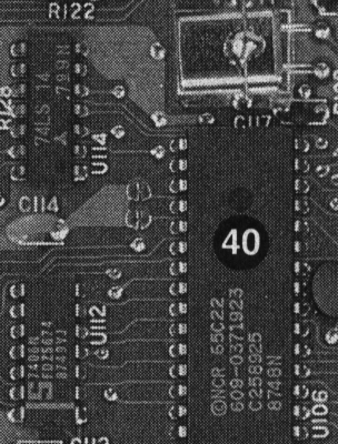
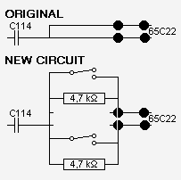
C128DCR INTERNAL DRIVE DEVICE NUMBER CHANGE:
The internal 1571 in the metal case USA version C128DCR has no external switches for drive select. It is factory set for device #8. There are drive select "jumpers" inside the computer however, on the motherboard near the drive. They are the two tiny silver half-circles with a bar between them. Cutting the bar opens the jumper. If you look at the PC board just under the left side of the drive, you will see them. It is not necessary to remove the drive unless you plan to solder in there. The jumpers are located near ICs U106 (a 6522), U114 and U112. DS (drive select) jumper #1 is nearest to U112, towards the front of the computer.
Electrically, the jumpers connect two pins of IC U106 VIA chip (65C22 or 6522 in some models) to chassis ground. Jumper 1 grounds pin 15 and jumper 2 grounds pin 16. That information is helpful just in case the foil pad(s) jumpers on the PC board are accidently damaged when you are installing a drive select switch. If the pads lift off the board, you can still make connections directly to the IC pins for your switch.
Look at pictures below: there's also circuit how to build device number switcher...
How can a turn my NTSC-M C64 into a PAL-B C64 or vice versa?
(is possible to apply also on commodore 128)
Changing a C64 from stock PAL-B to stock NTSC-M or vice versa requires swapping in the approproate VIC-II chip and the appropriate crystal, as well as changing a jumper on he motherboard (The jumper has printing near it that indicates whether to cut or connect the jumper). Also, if you have a version 1 KERNAL ROM and want to use the built-in RS-232 routines, you need to either swap KERNAL ROMs with the other computer (not recommended), or obtain a revision 3 KERNAL (recommended).
Now, if maintaining stock operation is not a complete must, or if you just want to tinker, the crystal and jumper modifications can be made optional. The VIC-II chip has a relaxed tolerance for timing, so it is possible to run an NTSC-M VIC-II with a PAL-B crystal and jumper settings. The converse is possible as well. Since the crystal freequency is used to generate the frequencies for the TV and monitor output, your TV or monitor may not like the resuling hybrid signal very well, but it won't break anything.
In addtion, the jumper indicated above determines the divisor used to scale down the crystal frequency for the CPU. For PAL-B units, the divisor is 18, and for NTSC-M units the divisor is 14. The Commodore 64 will operate regardless of the crystal frequency and state of this jumper. Therefore, to speed up a C64, one can install a PAL-B crystal (17734472Hz) and change the jumper to use the NTSC divisor (14) to increase the operating speed of the machine to 1266748Hz. However, note that any operations (disk, RS-232, special VIC tricks) that require synchronized timing may fail in this "non-stock" scenario.